


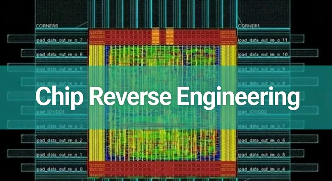
Chip Reverse design, in simple terms, is the process of extracting, analyzing, and organizing the internal circuits of a chip to achieve a deep understanding of the technical principles, design ideas, manufacturing processes, structural mechanisms, and other aspects of the chip. It can be used to verify design frameworks or analyze information flow issues in technology, and can also assist in new chip or product design solutions.
Sichi Technology has long been committed to providing technical support and services for design companies in product positioning, competitive research and analysis, copyright protection, and learning advanced design concepts and skills through cooperation with well-known chip design enterprises. We have our own unique technical and practical skills in chip reverse design. Our fast and accurate circuit reverse extraction, as well as efficient circuit collation and analysis, can provide customers with an independent innovation platform, thereby shortening the learning curve and accelerating the improvement of their own technical level.
|
|
Digital Circuits |
Analog Circuits |
|
Design Service Scope |
Standard cells, gate arrays, semi-custom and full-custom designs |
CMOS process and Bi-poly process |
|
Service Content |
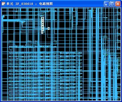
Provide two-level circuit schematics (top-level and cell-level/gate-level) as shown in the figure below. Circuit schematics can be generated according to layout placement; provide ERC checking and support SVS flow. |
Provide transistor-level netlists/circuit schematics, including geometric parameters such as transistor width-to-length ratio; generate circuit schematics according to layout placement; provide ERC checking and support SVS flow. |
|
Data Delivery |
Data formats: Verilog and EDIFDeliverables: Image data, raw netlist data, and two-level circuit schematics generated based on layout positions. |
Data formats: SPICE and EDIFDeliverables: Image data, raw netlist data, and circuit schematics generated based on layout positions. |
Our chip reverse design services include netlist/circuit schematic reverse extraction, hierarchical circuit collation, logic function analysis, layout extraction and design, design rule check and adjustment, logic-layout verification, cell library replacement, and process size scaling.
Through these reverse analysis methods, we can help clients understand the design of other products for project feasibility studies, open up ideas, identify problems, cost accounting, etc. For example, before entering a new field, we can evaluate and verify the feasibility of our technical solutions and design ideas; Assist in solving critical technical issues through research on mature products in the market; Utilize the market resources of existing products, reduce entry barriers, achieve better product compatibility, and so on.
Reverse extraction of netlist/circuit diagram
In the reverse design of chips, the extraction of netlists/circuit diagrams is a major issue, and the quality and speed of netlist extraction directly affect the subsequent organization, simulation, LVS and other aspects of work. Based on summarizing numerous successful cases and relying on independently developed software applications, we can accurately, quickly, and with high quality extract netlists/circuit diagrams.
Standard process for netlist extraction and functional analysis
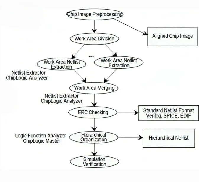
Logical Function Analysis
After the netlist extraction is completed, it is often necessary to organize the circuit by hibernating a flattened circuit to form a hierarchical structure of the circuit, in order to understand the designer's design ideas and techniques, and also to achieve the goal of finding netlist errors.
Logical Function Analysis 1
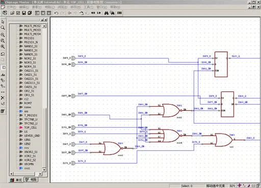
Logical Function Analysis 2
Layout design
Layout design is the physical implementation of circuit logic and is the implementation of integrated circuit products (ChipLogic Layer editor). We provide various design services such as layout extraction, process library replacement, target process modification, DRC inspection, and LVS verification based on reverse design. The service content is as follows:
|
Design Service Scope |
Digital Circuit |
Analog Circuit |
|
Standard Cell, Gate Array, Semi-custom and Full-custom |
COMS Process and TTL Process |
|
|
Service Content |
Extract top-level and cell-level layouts; Complete DRC check; Cell library replacement and process size scaling |
Extract top-level layout; DRC design rule check |
|
Data Delivery |
Data Format:GDSII; Provide image data, original layout data and DRC-passed layout data |
Data Format:GDSII; Provide image data, original layout data and DRC-passed layout data |
Standard Process for Layout Extraction and Functional Analysis
Logical layout verification
After the completion of netlist and layout design, various verifications of their correctness are often required. In order to ensure the integrity of the design process, Sichi Technology provides various verification services for chip netlist data and layout data.
|
1 |
FPGA Verification |
Verify the correctness of logic extraction by burning the chip |
|
2 |
Logic Simulation Verification |
Verify the correctness of logic extraction by writing test vectors according to the chip specification provided by the user |
|
3 |
LVS Verification |
Verify the consistency between the layout and the schematic |
Address:Room 302,RongXing Building,FuHao Garden,168# Road Bulong,Bantian Street,Longgang District,Shenzhen City,Guangdong,China.
SMT factory: 9th Floor, Hongji E-Valley, No. 23 Tongji West Road, Nantou Town, Zhongshan City, Guangdong Province, China.
Tel:+86 755 8304 8995
Fax:+86 755 8304 5278
Mob:+86 134 8015 1328
Copyright © 2012-2026 Shenzhen Sichi Technology Co.,LTD. Powered by iglobalwin.com